I am returning more and more to LM3900 implementation for circuit design electronic music circuit design. From on-going development, I've had several glimpses now of precision, performance, and temperature stability. And all of these traits operating from a single power-supply voltage, generally +15V.
I'm working on a new kind of ADSR envelope generator, one that will have programmable delay, some complex waveshape options, as well as flexible retrigger modes.
For the circuit design of this envelope generator, I wanted to see if I could have a more balanced range of up and down slopes in the integration, and also more dynamic range beyond what the LM3900 difference integrator could do (AN-72, Figure 83).
The difference integrator is particularly useful in closed-loop servo loops that use feedback to establish a condition. But it's dynamic range is limited, unless zeroing the input bias current technique is used (AN-72, Figure 84). But even then, the use of the +input for positive integration does not allow balanced rates, given the same input currents into both inputs. The alternative to this is to apply the voltage mirror circuit technique that uses the -input on two op amps to provide a more precise fulcrum on one of them (AN-72, Figure 69). This does work, but it is somewhat more complex, and has unbalanced control rate limits on the positive input side due to the necessary capacitive feedback loop compensation.
The Current Mode Amplifier (CMA) seemed like it might be a good starting point to form an integrator, because as a transconductance amplifier, it had good voltage compliance, and a wide range of available output currents. Because the CMA provides only a current source for charging a timing capacitor, the main question was how to provide a current sink and a switching means between them. This was made possible in the test circuit shown below, by way of adapting a current mirror and switching circuit developed in Dennis Feucht's Designing Waveform Signal Processing Circuits, p. 109.
The 2MΩ resistor provides the -input to opamp #3 with common-mode range compensation, to allow a 0-2.5V control voltage input with a 50K trimmer. The CMA circuit design centers on a ΔV = 2.0V, but this test arrangement allowed a little more range. Similarly, getting the output through the 2N5087 close to no current output for 0.0V input is accomplished by the other 50kΩ trimmer connected with the 180kΩ resistor, tied to +15V. More ideally, the +15V could be replaced by a different reference not subject to possible power supply variations, esp. as the zero adjust sets the longest dynamic range in this test circuit. However, as we'll see, some kind of non-linear control will ultimately be needed to set range (see note at end).
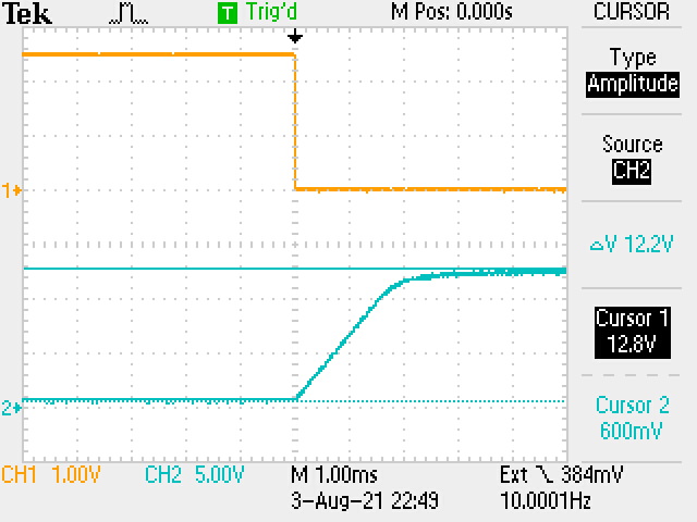
In contemplating this circuit originally with the LM3900 as the difference integrator, a DC offset for the lowest envelope voltage output was already anticipated. As it happens, between the current mirror and the saturated switch, the Vout|min is ≈0.6V, or ≈1Vbe. This can be taken out by a variety of means, including an output buffer, which was intentionally not included in the test circuit. Also, to note, the 10MΩ scope probe to the Tek TBS1064 scope will cause as much as ≈1μA of current to be drawn away from the current source, affecting timing accuracy for low current ranges.
Some scope fotos show how well the circuit works.
This integrator does work well, but it also has some issues. The control range for fast rising/falling slopes is quite constrained. For slower rates, the full dynamic range is set by the offset voltage provided by the 50kΩ trimmer intended to match the 0.00V input with the ±5% tolerance of the 1N5242B Zener diode that provides the +13V reference voltage via op amp #2. There is some play there, esp. as a single-turn trimmer likely provides inadequate trimming range for very small input control voltages that set the longest integration times.


Comments
Post a Comment